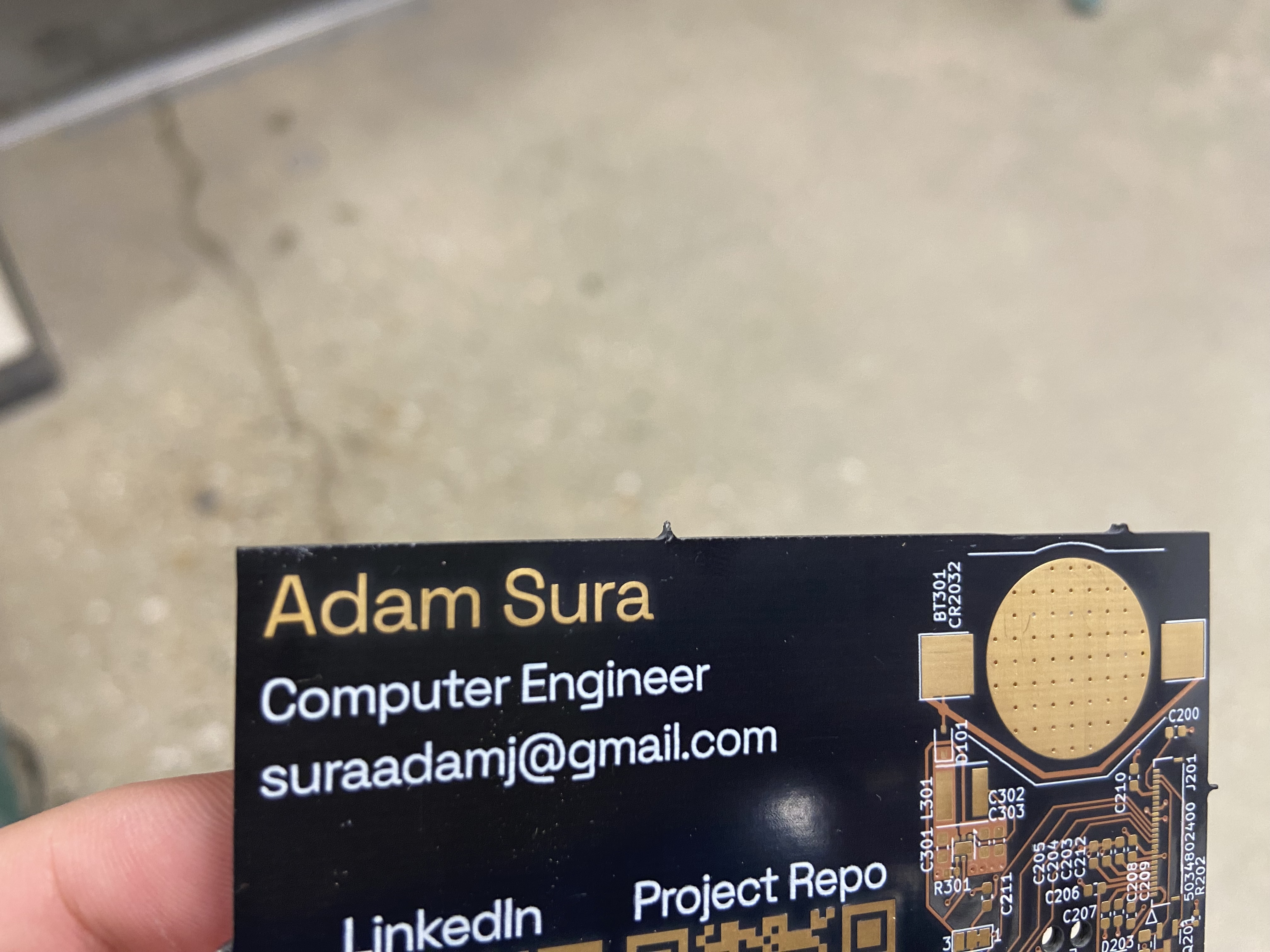
PCB Assembly
Once I had all of the parts ordered, it was time to assemble. This was my first time assembling SMD components by hand, so I had to learn how.
Reflow Oven
I decided early on that I wanted to solder the entire board all at once with a reflow oven instead of using a hot air gun on each part. I had seen online that many people build their own reflow devices using a toaster oven or skillet combined with an thermocouple, relay, and Arduino. In my ECE 203 class Spring 2025 semester, I designed and built one of these ovens using a toaster oven I bought from Saint Vincent de Paul's. It used an Arduino clone to control a solid state relay hooked up to the oven's heating elements. Internally, the code used PD+feedforward control to maintain a desired temperature with reference to a thermocouple. Despite the outward appearance of the oven, it produced very good results, leaving cleaner pads then the oven I used later on.
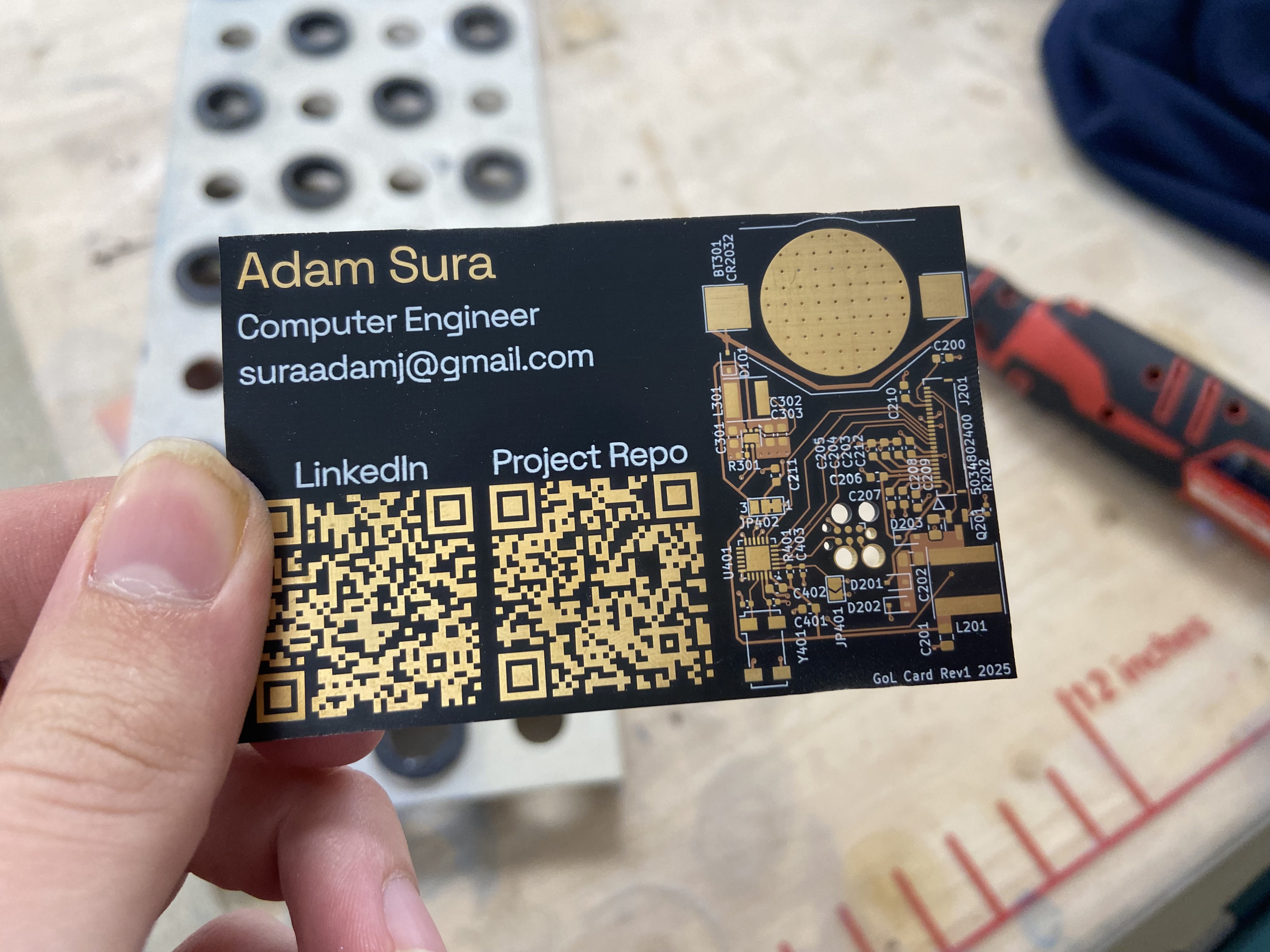
Board Assembly
Note: the pictures in this section are from the second batch of boards I assembled this September.
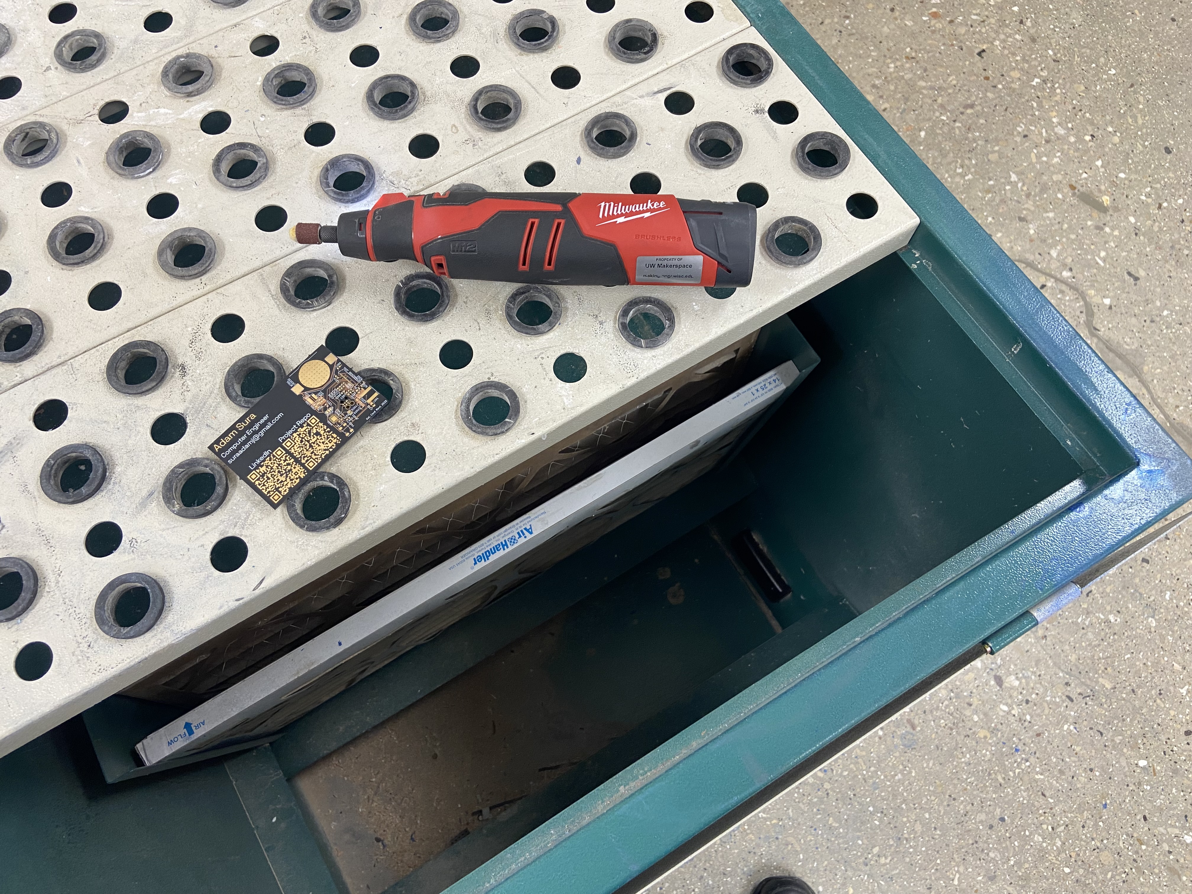
Once it was time to assemble the boards, I headed over to the UW-Madison Design Innovation lab for a place to work as well as access to a microscope. This microscope was crucial in the assembly process, and it would have been nearly impossible to complete this project without it.
The first step was to grind down the panelization spurs that came on my boards from the PCB manufacturer, who places multiple different boards from multiple orders on a single large panel for manufacturing.
I did this using a rotary tool with a sanding attachment. Since normal PCBs have a fiberglass based substrate in them, and microscopic fiberglass in the air could be harmful to breath, I used the tool inside a vacuum table in the lab's wood shop.
When grinding, I made sure to be liberal with the grinder to ensure the rest of the edge would be the high point on each board.
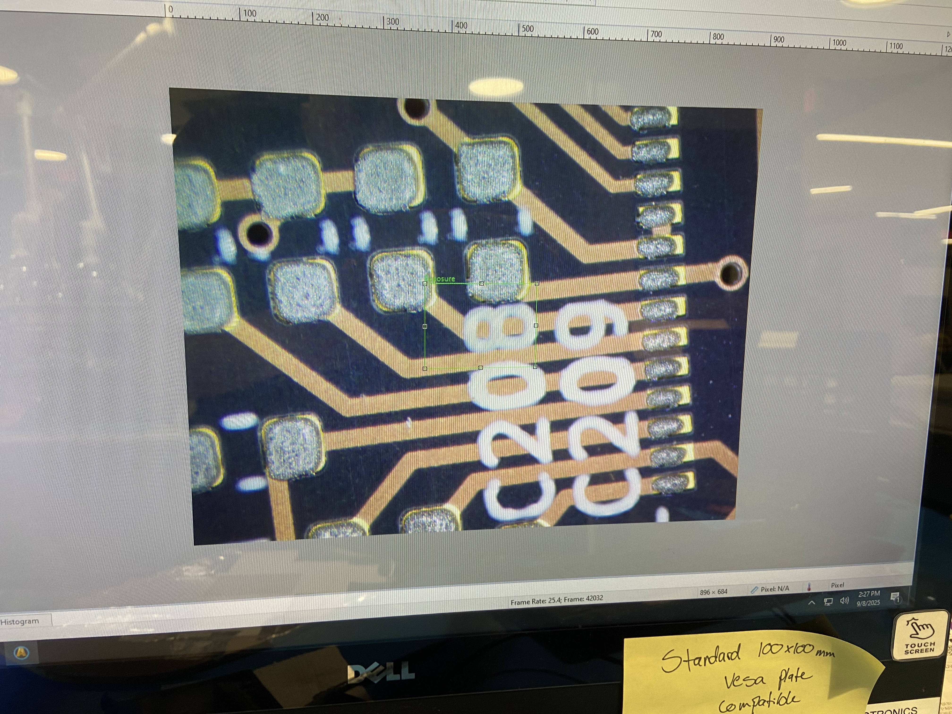
Once the boards had been ground down, the next step was applying the solder paste using the stencil. My first set of attempts to do this were not well thought out and resulted in many bridges between small pads. After watching this video about pasting, I used a similar process. I began by printing out four 90mm x 90mm x 1.6mm plates on the lab's 3D printers on a very low layer height preset along with ironing the top layer to make a plate very close to the thickness of a PCB. I taped these plates around one of my PCBs using thin tape to create a jig that would securely hold the PCBs during the pasting process. I then used some blue painter's tape to tape the stencil into place before (ideally) wiping down the board and stencil with isopropyl alcohol. After the surface was dry, I applied paste and used a putty knife to spread it across the stencil and board. I chose to pull the paste in the direction along the pins of the FPC connector, which were prone to bridging in my previous runs.
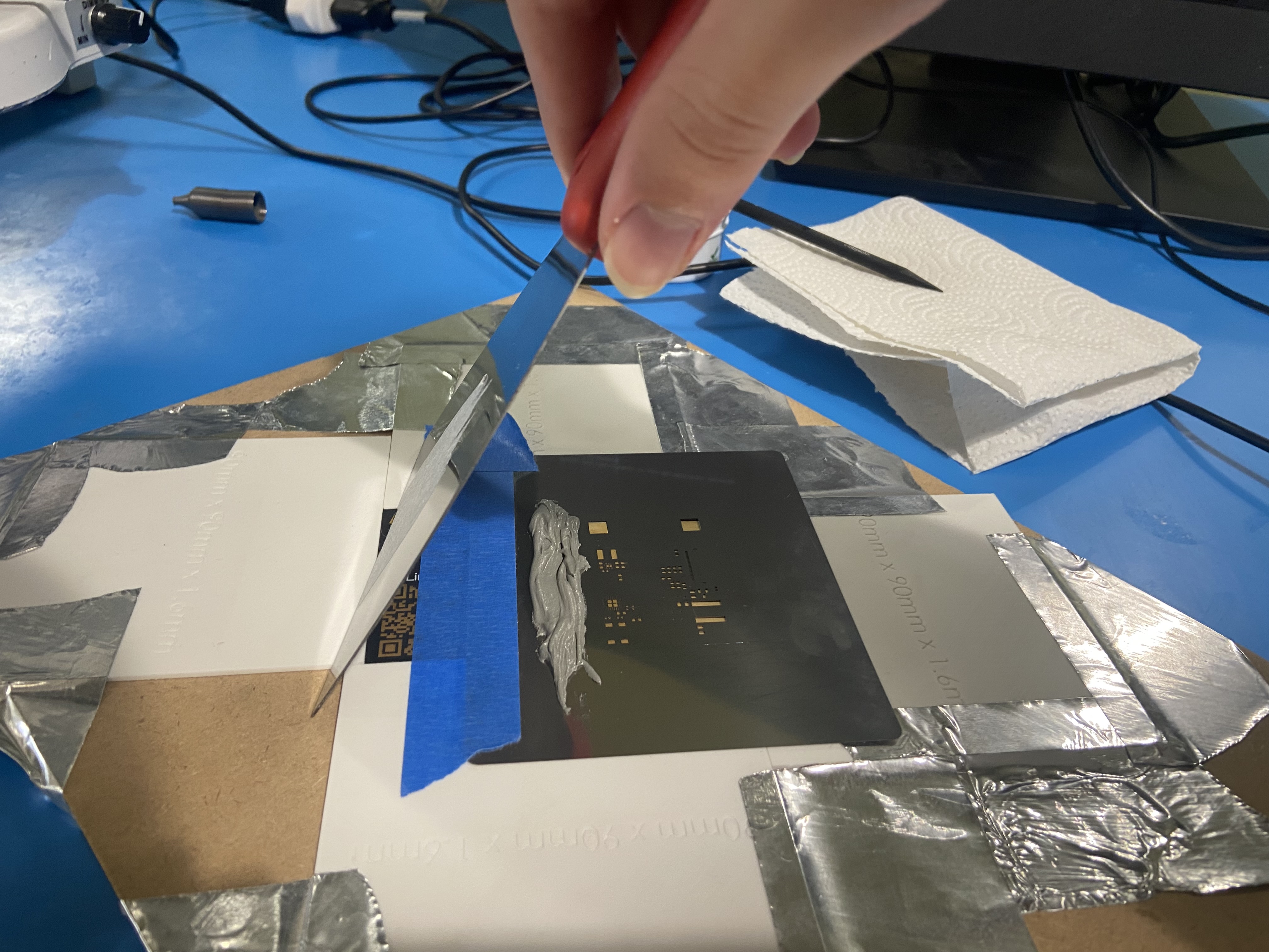
Before continuing, I inspected the boards to make sure the paste was in approximately the right position and did not have any bridges.
After this, it was time to assemble. There wasn't anything too special to this besides a pair of fine tweezers, a microscope, and a bit of patience. I had my KiCad project on my laptop to make sure I was grabbing the right components from my stack and putting them in the right place.
Reflow Soldering
The first board I produced I reflowed in my homemade reflow oven described above. However, that oven was very large and a bit difficult to use. The day that I was making the boards pictured above, someone came to my station to use two mini ovens that were right there on the table. I had seen these before, but I thought they
- were for PCB rework and not reflow, and
- didn't have the right settings for my solder paste.
However, I saw the person using the station to reflow a MOSFET onto a PCB, and the machine supported custom profiles. Since the PCBs and components should be able to survive at least two reflow cycles, I decided to give the new oven a try. I programmed the flow profile from my solder paste's datasheet into the machine, and did a dry run to verify it worked. After not seeing any issues with the profile, I placed one of my boards into the machine and fired it up. The resulting board looked a bit more scorched than the one I made in my own oven, but I was able was able to connect to it with my debugging probe, which will be discussed shortly. The remainder of the boards were then assembled using this oven.
Programming and Final Touches
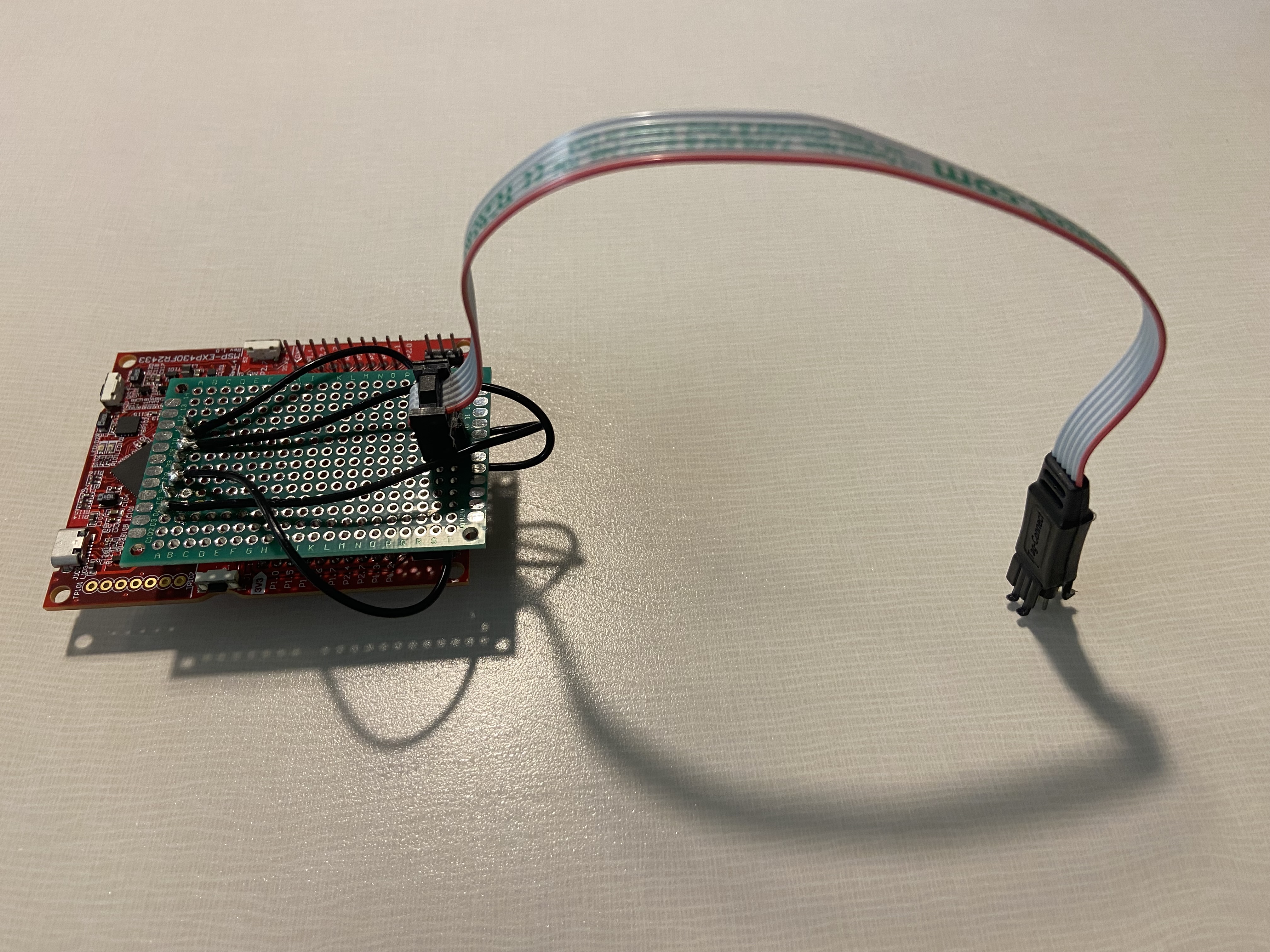
Once I had assembled boards, it was time to flash my firmware onto them. To do this, I created an adapter from the eZ-FET debugger on one of the Launchpads I had used during the first stage of this project to the Tag Connect cable that would attach to the board.
My first test consisted of connecting the board to debugger and using MSPDebug to see if the debugger could even connect to the board. After this, I would flash the code onto the microcontroller. I later starting doing a test at this stage that involved connecting an ePaper display to the board and making sure it reset to black, as the board is set by default to all zeros.
Once I had flashed the firmware, I used MSPDebug to flash the initial board state onto the chip. For my first few boards I reused the test state I had been working with in the simulator, but once I started really working on the boards I used the command line to generate a file full of random bytes (plus zeros for the "header") and flashed that. It was important that this was done now as once I soldered the jumper to the boost converter closed using the debugger would fry the boost IC, and desoldering the jumper would take a bit of effort.
If I was able to redesign the project with the knowledge I have now, I would replace the jumper with a SMT switch. This would be much easier to use that a solder jumper, provide better isolation between the debugger and the boost converter, and act as a reset switch removing the need for a second reset jumper near the MCU.
Once everything was programmed, I went and soldered the jumper to the boost converter shut to connect it to the rest of the board. Once I made sure everything worked with a coin cell, I used hot glue to attach the display to the back of the PCB. This is because it is easy to remove with isopropyl alcohol and it does not release fumes when heated like CA glue does. The downside is that the glue comes off fairly easily, but for something that I want to be easy to remove it is not a huge deal.